Scanning Tunneling Spectroscopy (STS) - Why it is useful and how simulations can help
- Mads Engelund

- May 21, 2024
- 5 min read
Updated: Jul 15, 2024
At a Glance:
Scanning Tunneling Spectroscopy (STS) is a technique performed with the same equipment as Scanning Tunneling Microscopy (STM).
STS is used when the STM image is too featureless to identify the atomic or molecular structure at a specific location.
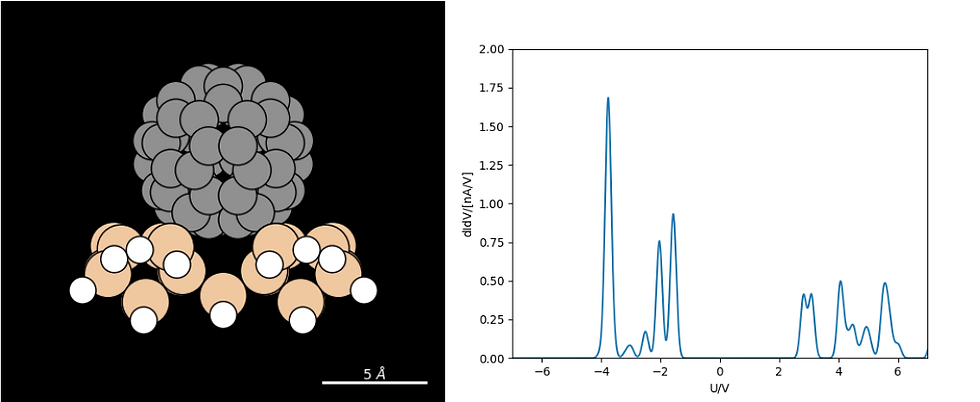
Under certain conditions, the derivative of the current with respect to the voltage (dI/dV) can be proportional to the sample's Local Density Of States (LDOS).
While dI/dV may not always approximate the sample LDOS well in complex situations, it still holds practical value for gaining insights into the underlying structure.
Achieving consistent dI/dV curves necessitates meticulous control over the tip's precise structure, highlighting the practical challenges of using STS.
Simulating STS in a system with a gap between occupied and unoccupied states requires a higher-level theory than density-functional theory (DFT) to approach any predictive power.

What is Scanning Tunneling Spectroscopy?
Scanning Tunneling Spectroscopy(STS) is a technique performed with the same equipment as Scanning Tunneling Microscopy(STM): a conductive tip and a conductive sample. If the STM image is too featureless to identify the atomic/molecular structure at a specific location, an experimentalist will typically use STS.
An experimentalist will typically perform STS in the following way:
Record a constant-current STM image.
Choose a point corresponding to the STM image's local maximum or minimum.
Hold the tip position constant while sweeping the voltage through a selected range of values.
Record the current for each voltage.
Repeatedly sweep the voltage values to improve the data collection statistics.
Unlike STM, STS does not produce an image but a current vs. voltage graph. Note that the experiment will still be a type of STS whether you plot the current directly, an "I/V curve," the first derivative, the "dI/dV curve," or higher derivatives.
dI/dV can Approximate the LDOS
Under some conditions, the derivative of the current with respect to the voltage, the "dI/dV," will be proportional to the sample's Local Density Of States(LDOS). The conditions are:
The voltage must be approximately constant in the tip and sample, so the voltage change only occurs in the gap between them.
The tip must have a constant LDOS near the Fermi Level.
The tip frontier electronic orbital must be approximately spherical.
So, the quintessential situation that would fulfill these conditions would be investigating small or flat molecules on top of a metallic sample with a metallic tip.
Departing from this simple situation with metallic tip and sample, the dI/dV spectrum becomes a poorer approximation of the LDOS. Let us imagine investigating C60 molecules on a Ge(001) sample using a Ge(001) tip functionalized with a CO molecule picked up from the sample. In this case, the voltage drop will occur over the tip, the gap, the C60 molecule, and the semiconductor surface. The CO molecule will distort the LDOS of the tip, and the pi-like frontier orbitals will pick out sample states different from those of a spherical orbital. In short, the recorded dI/dV will have little to do with the sample's LDOS.
dI/dV as a Fingerprint
While the dI/dV may not always approximate the sample LDOS in complex situations, it still holds practical value. By recording dI/dV, we can gain insights into the underlying structure we are investigating, whether a molecule, cluster, or defect. However, achieving similar dI/dV curves necessitates meticulous control over the precise structure of the tip, underscoring the practical challenges of using STS.
Using the dI/dV as a fingerprint in this way demands meticulous control over the tip. In STM operation, it is a common practice to "dip" the tip into the sample to pick up a small cluster at the end of the tip to enhance STM contrast. However, even slight variations in the formation of this cluster can lead to significantly different dI/dV spectra. A more reliable approach for consistent dI/dV is to pick up specific molecules prepared on the sample. Using dI/dV as a fingerprint of the underlying structure requires a high commitment to create a consistent experiment.
dI/dV Major Peaks
Another option exists if you cannot achieve the tip control needed to produce an entirely consistent dI/dV - focus only on the position of the most substantial peaks in the dI/dV spectrum.
The reason to focus only on the significant peak positions is that the experimental factors that affect the precise position are ones that you have complete control over—the semiconducting/metallic nature of the sample and tip and the macroscopic shape of the tip. The discrepancy between the LDOS and dI/dV peaks is sometimes called the Tip-Induced Band Bending (TIBB). On the other hand, the precise atomic termination, which is hard to control, will influence peak heights and shapes but have less power to change peak positions.
Using an analysis of the position of significant peaks in a dI/dV spectrum while ignoring the details of the spectrum can be an excellent way to identify molecules, clusters, and defects in your sample.
Simulating STS
Let us imagine the full complexity of a system with a semiconducting sample, tip, and bulky molecule as the feature of interest. In this case, getting an accurate simulation of the dI/dV would require using some multiscale approach. Considering the macroscopic shape of the tip, one could solve the voltage drop with electrostatic equations and couple this with solutions for the STM current, given a voltage drop over the tunneling gap.
Another challenge is that density-functional theory (DFT) level simulations tend to give extremely poor predictions of the gap between occupied and unoccupied states, which is unfortunate if we wish to use the relative peak position to identify features. We need a higher-level theory than DFT to approach any predictive power. One such method is the GW method, which can produce much more accurate occupied-unoccupied gaps—10-20 % error, rather than 100-200 % for DFT-level calculations.
A final challenge is determining the tip's position when you perform a dI/dV sweep. Theorists mostly pick a tip position near the feature of interest with little further thought, but the position can be significant. However, for the best simulation results, the tip position should be chosen by emulating how the experimentalist initially chose it.
Simulation Support
At Espeem, we have chosen to support STS experimental work on semiconductors in the following way:
Correct the occupied-unoccupied gap with GW calculations. These calculations are costly in computation time, but DFT-level calculations are insufficient.
Pick the tip position based on experimental workflow. As standard, we always perform an STM simulation and then pick the tip position based on an image feature, usually the maximum. We perform the STM and STS simulations with consistent parameters.
Disregard the voltage drop in the tip and sample for now. For a similar tip, sample, and underlying structure, the voltage drop should result in a similar expansion, which we can correct for.
I hope this quick review of the STS method has helped. If you would like us to examine your STS challenge, explore our offer to create STM/STS-based simulations for you.


Comments